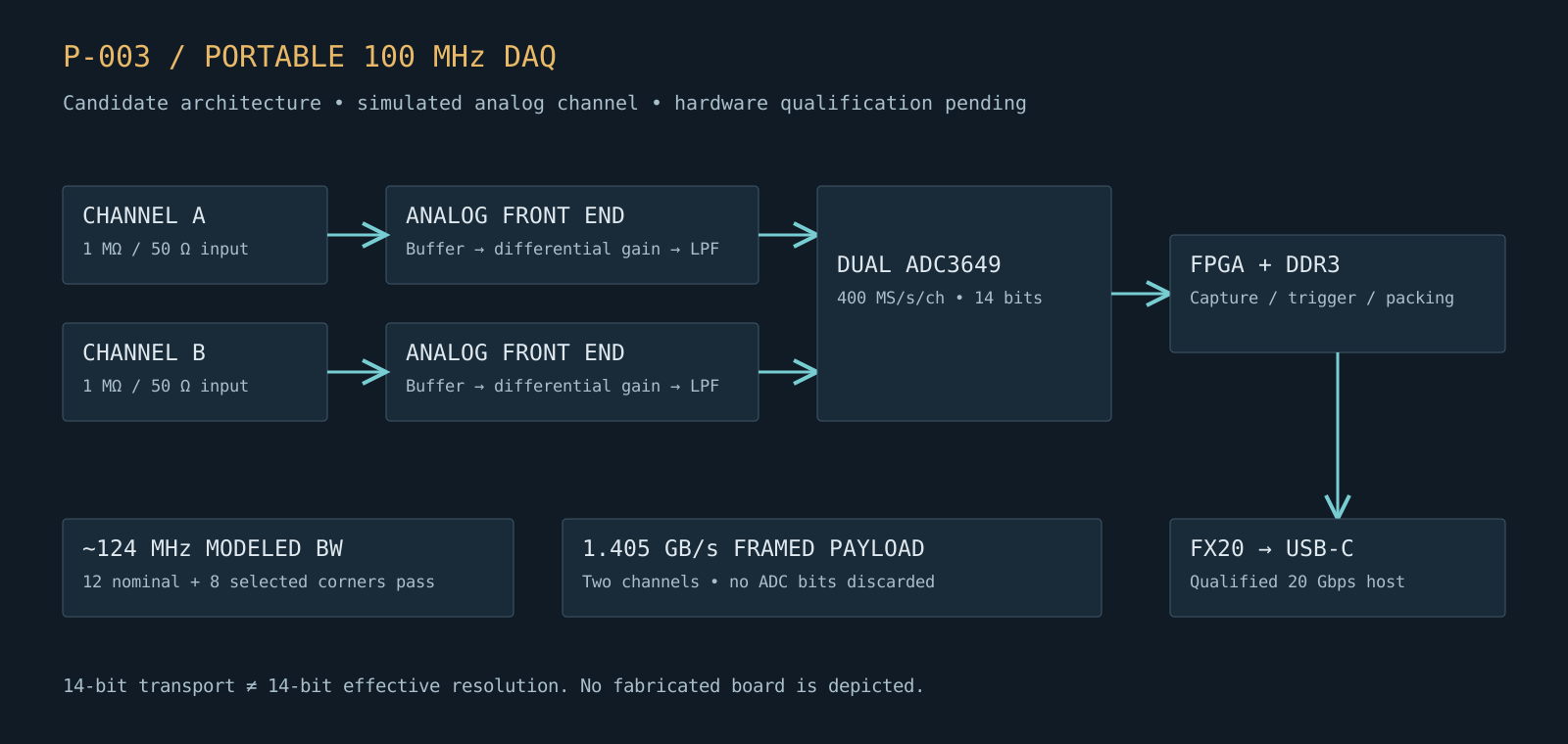
A portable two-channel acquisition instrument, designed around 100 MHz analog bandwidth and USB-C. The current candidate retains all 14 ADC bits at 400 MS/s per channel, with a documented simulation trail and explicit limits on what those simulations establish.
Fig. 1 — Candidate architectureThe proposed instrument: two simultaneous analog channels and a shared acquisition path. This is an architecture diagram, not a fabricated board or a completed hardware schematic.
01Overview
What it is
The project began when the LTspice automation tool was mature: choosing a real acquisition architecture, turning its analog path into executable netlists, and checking the decisions against saved waveforms. Each channel uses a compensated range divider, a high-impedance buffer, differential amplification, programmable gain and a passive anti-alias filter ahead of a dual ADC.
The development baseline is 400 MS/s per channel. Two channels at 14 bits generate 1.4 GB/s before framing. That points toward an FPGA and FX20 bridge on a qualified USB 20 Gbps host, with memory for triggered acquisition and host stalls. USB-C describes the connector; it does not guarantee that a particular computer can sustain this stream.
This is a design in progress. The evidence covers a representative analog channel with vendor macro-models and an approximate ADC input load. It does not yet establish two-channel crosstalk, converter SINAD, USB throughput or finished-board performance.
02Capabilities
What it does
Analog candidate
OPA817 → LMH5401 → LMH6401 → nine-pole differential filter, evaluated across input ranges and gain settings.
Traceable results
Generated netlists, simulator logs, RAW waveforms, script snapshots and hashes identify exactly what produced each result.
Tolerance studies
Eight selected corners and 64 seeded L/C variations test response margin within declared assumptions.
Transport budget
A lossless 14-bit packing reference and explicit host, buffer and memory-bandwidth calculations.
03System design
How the schematic earns bandwidth above 100 MHz
Start with three separate requirements: preserve the 0–100 MHz signal band within ±0.5 dB, put the −3 dB cutoff above 100 MHz, and reject signals that would alias into the retained band. A part labeled 100 MHz cannot satisfy all three by itself. The connected circuit, its loads, sampling clock and physical layout must be designed together.
The current synthesis uses a 125 MHz low-pass filter and 400 MS/s per channel. The saved analog model reaches about 123.81 MHz at −3 dB; this is connector-referenced and excludes the external probe. The walkthrough below separates retained simulation evidence, an interactive ideal-filter calculation, and parameters that still need PCB extraction or bench qualification.
A / Design the complete transfer function
Bandwidth is earned at every stage
01 / Preserve the input
Compensated divider
A high DC resistance is not a high RF impedance. Probe, relay, clamp and pad capacitances load the source and change divider compensation.
Rt × Ct ≈ Rb × Cb,total
100:1 model: 990 kΩ × 2 pF = 10 kΩ × 198 pF. The bottom total includes buffer/protection capacitance; the external probe is not modeled.
02 / Isolate the divider
OPA817 follower
The FET-input buffer separates the high-impedance divider from the low-impedance differential stage. Closed-loop flatness, input capacitance and large-signal response matter together.
Unity gain · ±6 V rails
TI lists 800 MHz small-signal and 250 MHz large-signal bandwidth at 2 Vpp. Neither is the bandwidth of this complete channel.
03 / Allocate gain and swing
LMH5401 → LMH6401
Convert to differential, then set gain without clipping an intermediate stage. Feedback resistors, noise gain, source/load impedance and common-mode control change the usable response.
~2.80 V/V at nominal code 21
1:1 connector-to-ADC DC gain. A 0.3 V peak input gives ~0.84 V differential peak before overshoot. Higher gain needs a smaller input.
04 / Shape the bandwidth
Nine-pole low-pass
A 125 MHz synthesis cutoff leaves the 100 MHz band relatively flat. More poles steepen rejection but increase component sensitivity, ringing and layout complexity.
~123.81 MHz modeled −3 dB
Seven poles miss the saved rejection check. Nine pass, with ~14.5–16.4% step overshoot. Bessel-like shaping favors pulse fidelity; elliptic zeros trade ripple and sensitivity for selectivity.
05 / Sample the signal
ADC3649 + clock
The converter needs enough analog input bandwidth and sampling speed. Its buffered input still requires a real drive/settling model and a quiet reference and clock.
2 Vpp differential · 1.4 V CM
The LTspice endpoint is only a 100 Ω || 2 pF load. It does not simulate conversion, clock jitter, sampling kickback or silicon distortion.
06 / Move and power the data
FPGA → DDR3 → FX20
Sampling faster relaxes filtering, but grows traffic, FPGA activity and thermal demands. Memory absorbs finite stalls; it cannot fix a persistent throughput deficit.
1.4 GB/s payload at 400 MS/s
512 MiB holds ~335.5 ms in 16-bit containers. Input power is ~9.1 W estimated / 14.0 W allocated; USB-C power and USB 20 Gbps service need qualification.
Do not add bandwidth ratings
Loaded stage responses multiply; their gains in dB add. As a teaching example, three isolated, identical 100 MHz single-pole stages produce only ~51 MHz combined −3 dB bandwidth. Real feedback stages are more complex: simulate the connected circuit with its terminations.
Htotal(f) = Hdivider × Hbuffer × Hgain × Hfilter
Small-signal bandwidth is only one test
A sine needs a peak slope of 2πfVpk. At 100 MHz and 0.3 V peak that is ~188 V/µs at the buffer. Check slew, output current, headroom and distortion at each stage, then verify step overshoot and settling. A flat AC sweep alone cannot establish a full-scale input rating.
Input example: 10 pF has |Xc| ≈ 159 Ω at 100 MHz, even when the port is labeled 1 MΩ at DC. The external 10×/100× probe, cable and compensation therefore need their own end-to-end bandwidth check.
Fig. 2A — Bandwidth through the chainRead in numbered signal-flow order. Component ratings explain the choices; connected-circuit simulations establish the quoted model response. No individual stage rating is an instrument specification.
B / Sampling buys filter transition room
Move the alias band. Watch the data bill.
Keep a 0–100 MHz signal band. The first higher-frequency band that folds into it starts at sample rate minus 100 MHz. Raising the sample rate moves that boundary away; raising the filter cutoff improves flatness but weakens rejection.
110 MHz · more rejection150 MHz · flatter
Swipe the chart to see the full frequency axis →
Teal shading: retained 0–100 MHzGold shading: first alias bandGold dot: ideal −3.01 dB cutoffDashed horizontal: −60 dB target
Droop at 100 MHz
0.078 dB
Within illustrative 0.5 dB limit
Rejection at 300 MHz
68.4 dB
Ideal edge clears 60 dB
Two-channel payload
1.400 GB/s
14 bits retained; before framing
Required host service
1.653 GB/s
Framing + 15% spare service time
400 MS/s is the compromise: the alias band starts at 300 MHz and the host target is about 1.653 GB/s. Actual host/controller/cable performance still needs qualification.
Analytical teaching model, not new LTspice results. A(f) = 10 log₁₀[1 + (f/fc)¹⁸]. No amplifier loading, loss, parasitics or distortion is included. At 125 MHz cutoff, ideal droop is about 0.078 dB; the saved full chain is about 0.267 dB down at 100 MHz. Its stopband can rise again because of feedthrough. A single ideal edge value does not verify the complete 300 MHz–1 GHz stopband.
The retained band is a processing choice, not the whole Nyquist band. A digital low-pass filter is still required before decimation; it cannot remove signals already aliased into 0–100 MHz. Neither decimation nor sample rate alone increases analog bandwidth.
Fig. 2B — Explore sampling and filteringChange sample rate and ideal cutoff to see transition room, passband droop and transport cost. This analytical illustration does not alter or rerun the retained LTspice studies.
C / Make physical assumptions visible
The board becomes part of the filter
These are the present netlist placeholders and unmodeled effects. They are not fabrication tolerances or released PCB constraints.
Use actual part values, frequency-dependent loss and vendor models; add pad/via/trace parasitics. Q at one frequency is not broadband qualification.
Filter input-to-output bypass
Sensitivity tested
Cfeed = 1 fF per leg nominal. Saved sweep: 0, 1, 5, 10 and 50 fF.
Extract capacitive and magnetic coupling. Keep input/output physically separated and return paths controlled. 1 fF is an assumption, not a proven layout budget.
ADC loading and drive
Lumped approximation
Rdiff = 100 Ω; Cdiff = 2 pF.
Check actual ADC impedance versus frequency, driver settling, reference loading and sampling effects. Validate at the selected clock rate and amplitude.
Routes / differential balance
Not yet modeled
ΔCpad, Lvia, trace delay, impedance error and mutual coupling: TBD.
Choose stackup and extract routes before assigning numeric limits. Include leg mismatch, return inductance, two-channel crosstalk and timing skew.
Integrate clock phase noise for the actual mode; include supply ripple/spurs, coupling, reference noise and thermal drift. Avoid counting aperture jitter twice.
Margin is finite. The worst selected corner is −0.4549 dB inside a −0.5 dB flatness limit: only ~0.045 dB remains there. Its −3 dB bandwidth still exceeds 118 MHz. Bandwidth margin therefore does not imply comfortable flatness margin for added PCB effects.
Closure sequence: select real parts → include their parasitics and loading → sweep corners and imbalance → extract the PCB → repeat AC/noise/transient checks → measure the board. Preserve a continuous reference plane with controlled current returns; set stackup and routing constraints from the actual interfaces.
Fig. 2C — PCB assumptions and closureModeled placeholders, a saved coupling sensitivity sweep and unmodeled board effects are explicitly distinguished. Values marked TBD are not validated routing or fabrication constraints.
D / Converter decision · reviewed 7 September 2026
Keep ADC3649 as the working baseline
Its dual 500 MS/s capability permits the 400 MS/s compromise, with buffered analog inputs, 1.4 GHz input bandwidth, LVDS output and about 0.6 W total typical converter power at 500 MS/s. The 1.4 GHz input specification is not the instrument bandwidth—and it makes an external anti-alias filter essential.
The 16-bit alternative improves these converter-only typical figures by ~1.8 dB, not the ~12 dB implied by two ideal extra bits. Its 14.3% traffic increase narrows host margin. A 250 MS/s alternative such as AD9643 lowers traffic but brings the first alias boundary down to 150 MHz, requiring a different filter strategy. Neither is a drop-in system improvement.
Bandwidth is not effective resolution
The saved front-end model contributes ~207–210 µV RMS at the ADC differential input over 10 Hz–100 MHz at nominal gain. Converter noise, folded noise, clock error, supply noise and distortion remain additional terms. Gain can overcome downstream noise but also clips sooner; bandwidth limiting can reduce noise but cannot retain signals it filters away.
Jitter grows more costly with frequency
SNRjitter = −20 log₁₀(2πfinσt). At 100 MHz, 100 fs RMS gives an ~84 dB jitter-only ceiling; 200 fs gives ~78 dB. These are ceilings, not total SNR. Add independent noise powers, and do not add aperture jitter again to measured ADC noise that already includes it.
Decision gate before freeze: measure or credibly budget SINAD/SFDR at 100 MHz and intended amplitudes, close the AFE noise budget, verify ADC drive/reference/clock behavior, and prove FPGA capture plus sustained FX20 service. Revisit ADC3669 if the resolution target justifies the extra traffic after those budgets close. The current evidence does not support 14 effective bits across the full band.
Fig. 2D — Why this converterADC3649 remains the development choice. Manufacturer specifications and calculated traffic explain the trade; the ADC is not yet qualified as part of a fabricated instrument. Host calculations retain every output bit and use the documented packet framing and 15% service margin.
04Frequency response
Margin above 100 MHz
All 12 nominal range/gain cases meet the proposed bandwidth, flatness and rejection checks. The complete modeled chain reaches about 123.81 MHz at −3 dB. Its worst relative gain at 100 MHz is −0.2672 dB, and minimum attenuation across the checked 300 MHz–1 GHz stopband is 69.28 dB.
At 400 MS/s, 300 MHz is the first frequency above Nyquist that folds into the retained 0–100 MHz band. The filter target is at least 60 dB attenuation over 300 MHz–1 GHz. These are engineering study thresholds, not a released instrument specification.
Fig. 3 — Nominal responseTwelve full-chain cases pass. The seven-pole passive comparison fails the rejection target; the nine-pole candidate passes. Gain is normalized at 1 kHz and referenced to the connector, excluding external probe loading.
05Tolerance
The response survives the variations tested
All eight selected corners pass, with bandwidth from 118.89 to 128.66 MHz and a passband envelope of −0.4549 to +0.1728 dB. The separate seeded study varies each inductor uniformly by ±5% and each capacitor by ±2%: all 64 cases pass, with minimum rejection of 68.04 dB.
The corner combinations are selected, not exhaustive. The 64-run study varies L/C only, with other assumptions held nominal. Neither result is a production-yield guarantee, and synthesized component values still need replacement with actual part models.
Fig. 4 — Seeded L/C variation64 saved runs, replotted from their RAW data. The dotted lines mark the −0.5 dB passband and −60 dB stopband checks. No physical production units were measured.
06A useful failure
A few femtofarads can bypass the filter
A filter can look excellent until the model includes a path around it. Adding 1 fF of input-to-output coupling per differential leg leaves 66.76 dB minimum rejection in the passive study. At 5 fF, that falls to 52.79 dB. At 50 fF, it is only 32.81 dB.
This simplified path is a sensitivity experiment, not an extracted PCB. It makes a concrete layout requirement: the stopband cannot be signed off until component parasitics, return paths and coupling are modeled and measured. The nominal circuit assumes 1 fF; that has not been demonstrated on a board.
Fig. 5 — Corners and bypass couplingThe rising high-frequency traces expose the coupling failure. Three coupling cases miss the rejection target and remain part of the evidence, rather than being removed from the result set.
07Time domain and noise
Keeping the waveform inside the converter range
Four input-mode pulse tests and four 100 MHz sine tests remain inside the modeled ADC voltage limits. Step rise times are about 3.89–4.05 ns, with 14.5–16.4% overshoot. The selected transient study uses a documented numerical convergence setting; invalid earlier outputs are excluded.
Retaining every ADC bit does not deliver 14 effective bits at 100 MHz. At the nominal gain setting, modeled front-end noise is approximately 207–210 µV RMS over 10 Hz–100 MHz. Maximum gain raises it substantially. Converter noise, jitter, alias-folded noise and distortion still have to be included, and the macro-model harmonics are not accurate enough to claim system SFDR or SINAD.
Fig. 6 — Pulse and sine responseCommon mode is the average of the two ADC input voltages and remains near 1.4018 V. Dashed lines show the ±1 V differential full-scale limits and 1.3–1.5 V common-mode range. Declared source amplitudes exercise the selected ranges; the external probe is not modeled. This checks signal excursion and step response, not protection or overload recovery.
08System tradeoffs
Why 400 MS/s is the working baseline
400 MS/s × 2 × 14 bits
1.400 GB/s payload / 1.405 GB/s framed
Host qualification target
1.653 GB/s for 15% spare service time
500 MS/s with the same margin
2.067 GB/s — buffered-mode candidate
512 MiB at 400 MS/s
~335.5 ms in 16-bit memory containers
Power estimate / allocation
9.1 W / 14.0 W input; qualification pending
The Python packing reference checked 131,072 sample codes, including every signed 14-bit value in each packing position, against an independent decoder. That verifies the proposed byte format. The FPGA capture path, memory controller, FX20 firmware and host software are still implementation work.
The upper voltage target is 300 V at an appropriately rated 10×/100× probe tip on isolated low-energy circuitry. That corresponds to 30 V or 3 V at the connector, respectively, with frequency derating still to be defined. It is not a 300 V direct-input or 50 Ω termination rating.
09Editable schematic
The circuit behind the curves
The candidate analog channel now exists as an editable LTspice schematic. All 52 elements match the native exported netlist after parameter substitution and instance-name normalization. Its finite AC response agrees with the selected reference to within 0.000001 dB across the saved sweep.
The images below are direct screen captures from LTspice: the editable schematic in its native editor and the saved simulation data in its waveform viewer. Application titles and controls are retained. Named nets connect separated schematic sections, while the differential filter is explicitly wired.
Fig. 7 — Native LTspice schematic editorCaptured directly from a larger LTspice window at 2780 × 1700 pixels, with the verified .asc open. This is the real editable 52-element candidate analog channel, not a redrawn illustration. Click to expand; the application window and exact source parameter declarations are retained.Fig. 8 — Native LTspice waveform viewerThe actual saved RAW result displayed by LTspice, captured at 2780 × 1700 pixels. Solid green is connector-to-ADC magnitude; dotted green is phase on the right axis. The roughly −31 dB passband includes the selected 100:1 divider and gain code 21. Earlier response figures normalize that passband to 0 dB; this native view shows absolute gain.
Not yet a PCB release
The schematic conversion is verified. The next circuit work is real protection/relay parts, filter components and power circuitry. FPGA bank assignment, timing closure and measured USB, thermal, noise and distortion performance remain design-freeze gates.
The selected evidence set contains 114 finite runs with matching artifact hashes: 110 meet their recorded checks and four negative controls fail rejection. Noise cases only check that modeled noise is finite and positive. This count is not a claim that 114 hardware performance tests passed.
Go read the source
The LTspice automation engine used for this study is public. The DAQ design package and hardware are still under development; this link opens the simulation toolkit, not a released DAQ repository.